

Published on Nov 30, 2023
SOI stands for silicon on insulator. This technology offers the possibility of building electronic devices in a thin layer of silicon that is electrically isolated from the thick semiconductor substrate through the use of a buried insulating layer.
In the standard silicon technology the semiconductor substrate is associated with undesirable effects such as high leakage currents, parasitic bipolar components, and, more importantly, interference between individual active devices or circuits built in the same integrated chip.
In addition, the use of SOI technology in CMOS (complementary metal oxide semiconductor) circuits may also shrink the dimensions of MOSFET (metal oxide semiconductor field effect transistor) devices and further push the frequency limit of silicon technology. The first confirmation that SOI technology is becoming the state-of the art technology in low-power IC's came in 1999, when IBM launched the first fully functional SOI mainstream microprocessor. The IBM specifications predict a 25-35% improvement over similar bulk CMOS technology, which is equivalent to about two years of progress in bulk CMOS design and fabrication. Besides the fast speed, other benefits of the new SOI chip are reduced power consumption (up to 3 times) and a small soft error rate.
While SOI has already become a mature technology for low power CMOS circuits and justifiably represents the main manufacturing technology for the next generation of ULSI (Ultra Large Scale Integration) low power circuits, it is still an emerging technology for high voltage power integrated circuits. An increased effort is now directed towards developing advanced SOI power device structures for integrated circuits. Compared to bulk junction isolated (JI) devices, SOI devices and circuits offer improved isolation, reduced leakage currents and faster switching speed. Nevertheless, power devices made in SOI technology may suffer from reduced breakdown levels, self-heating effects and latch-up. Several solutions to address these drawbacks partially or totally have been proposed in this paper.
This paper gives an introduction to SOI technology and devices, reviews major steps in developing SOI power devices for integrated circuits, discusses advantages and drawbacks of SOI devices compared to bulk silicon devices and finally reveals the most recent developments in high voltage SOI structures.
Creating defect free films of single crystal silicon on an insulating layer is a technological challenge. Several techniques have been developed to do this, but of these only a few have been commercially successful: silicon-on-sapphire (SOS), separation by implantation of oxygen (SIMOX), bonded and etched back SOI (BESOI) and uni-bond wafers produced by the smart cut process. Each of these in turn are discussed briefly:
Until the 1980's silicon-on-sapphire was the Most mature of all SOI materials. It is produced by growing thin films of single crystal silicon on a sapphire wafer by chemical vapor deposition from silane gas at 1000°C. such films have the advantage of lying on a substrate which is extremely good conductor of heat; also they are highly immune to radiation. However, cost of silicon-on-sapphire material, the relatively poor quality of silicon films, and the emergence of new SOI technologies such as SIMOX and wafer bonding which are based purely on silicon have prevented it from becoming a mainstream SOI technology; its use remains a niche market.
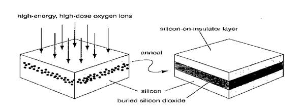
Although the concept of separation by implantation of oxygen (SIMOX) has been known since the 1970’s, it was only when a high current oxygen implanter became available in 1985 that SIMOX technology became a serious contender to SOS. To make SIMOX SOI wafers, a silicon substrate wafer is implanted with a high dose of oxygen ions at a high energy (1.8 x 1018 cm-2 at 150-200 Kev is typical) and is then annealed at 1300-1350°C for several hours; this is shown schematically in Fig.1. Under these conditions, the silicon layer and oxide layer is typically 200nm and 400 nm thick, respectively but with modern SIMOX process a top silicon layer as thin as 50nm and a buried oxide layer of thickness 100 nm are feasible.
Another modern technique for manufacturing SOI wafers is wafer bonding. The basic technique is shown in Fig.2 and relies on the fact that polished and flat wafers, when brought into contact at room temperature, are attached to each other by Van Der Waal’s forces and bond. To strengthen the ‘bond’ between the two wafers, a post bonding anneal at high temperature is usually performed and the top silicon wafer is then polished to create a thin silicon on insulator layer suitable for device manufacturing. However the uniformity can be improved by using wet-etches that are selective and will stop on a suitably placed etch stop layer of p¬+ silicon. Such techniques are known as bonded and etched-back SOI (BESOI).
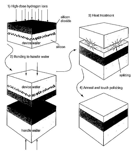
Alternatively, bonded wafers with silicon-on-insulator layers that are extremely uniform can be manufactured using the smart-cut method. This is shown in Fig.3. The device wafer, which has a layer of silicon dioxide on top of it, is implanted with a high dose of hydrogen ions (between 3.5 x 10¹⁶ and 1 x1017cm-2), after which it is bonded to the handle wafer which requires only a final high-temperature anneal and touch anneal and touch polish to yield the finished wafer. Versatility is the key advantage of the smart-cut method, as it can be used to create SOI wafers with buried oxide thickness from 200 nm to 4 nm, and silicon thickness from 200nm to 1.5μm12.
Historically, the SOI technologies were developed as a solution to parasitic effects (such as the generation of a current by photo-ionization) noticed in thick substrates when a wafer was exposed to radiation. Today SOI technology is considered the most promising technology for monolithic integration of CMOS and bipolar devices. Besides immunizations from ionization by atoms and radiations the SOI technology provides several important advantages, such as reduced parasitic capacitances, short-channel effects, hot-carrier effects and static consumption.
But the most important feature that establishes the SOI technology as a strong option for next generations of ULSI circuits is that it provides perfect isolation between individual device cells. Bulk circuits use reverse biased junctions to isolate individual devices from the substrate or /and from one another .for this reason the bulk technology in the high voltage field is commonly preferred to as junction isolation (JI) technology .the use of reverse biased junctions as isolation means has major drawbacks, such as increased parasitic capacitances and high leakage currents. Further more latch up structures such as npnp parasitic thyristors present in bulk CMOS inverters are completely eliminated in SOI technology. But there are still some problems associated with the SOI technique, such as floating substrate affects and self-heating, which will be addressed.
When the gate source voltage is greater than the threshold voltage an inversion layer is formed at the surface, which allows transport of electrons from the source to the drain. The MOSFET can be turned of by lowering the gate voltage below the threshold voltage .the on state resistance of the MOSFET in the linear region is proportional to the length of the inversion layer and the thickness of the gate oxide and inversely eruptional to the difference between the gate voltage and the threshold voltage and the mobility in the inversion layer.
When the drain voltage reaches a certain level, termed the saturation voltage, the condition for strong inversion is no longer satisfied and the inversion layer is pinched of at the drain side. This leads to current saturation .the main difference between SOI and bulk transistors is that the former is dually controlled by front and back gate bias. The two gates indices two depletion regions (fig 4) and, this gives rise to the following classification of SOI MOSFET structures
| Are you interested in this topic.Then mail to us immediately to get the full report.
email :- contactv2@gmail.com |
